AI computer maker Graphcore unveils 3-D chip, promises 500-trillion-parameter ‘ultra-intelligence’ machine | ZDNet
Graphcore, the six-year-old, Bristol, England-based maker of artificial intelligence chips and systems, on Thursday announced a new chip called “Bow” that makes use of two semiconductor die stacked one on top of the other, which it said will speed up applications such as deep learning training by forty percent while cutting energy use.
The company also announced updated models of its multi-processor computers, called “IPU-POD,” running the Bow chip, which it claims are five times faster than comparable DGX machines from Nvidia at half the price.
In a nod to the increasing model size of deep learning neural nets such as the Megatron-Turing, the company said it is working on a computer design, called The Good Computer, which will be capable of handling neural network models that employ 500 trillion parameters, making possible what it terms super-human “ultra-intelligence.”
The Bow processor is the latest version of what Graphcore refers to as “IPUs,” standing for Intelligence Processing Units. The company has previously released two iterations of IPU, the last one being in late 2020.
Bow, which is named for the Bow neighborhood of London, is “the first step in what to us is a strategic direction that involves vertical silicon integration, in other words, stacking silicon dies on top of each other,” said Simon Knowles, co-founder and chief technologist of Graphcore, in a media briefing.
Also: ‘It’s fundamental’: Graphcore CEO believes new kinds of AI will prove the worth of a new kind of computer
Similar to the “Wafer Scale Engine” developed by competitor Cerebras Systems, the Bow makes use of novel manufacturing techniques that go beyond conventional microprocessor fabrication.
The Bow is the first chip to use what’s called wafer-on-wafer chip technology, where two die are bound together. It was developed “in close collaboration” with contract chip manufacturing giant Taiwan Semiconductor Manufacturing, said Graphcore’s CTO, Simon Knowles, in a briefing for media.
The chip can perform 350 trillion floating point per second of mixed-precision AI arithmetic, said Knowles, which he said made the chip “the highest-performing AI processor in the world today.”
Cerebras’s WSE-2 chip appears to be faster than that, according to an estimate by the technology newsletter Microprocessor Report, which claims the WSE-2 delivers as much as 1,700 to 3,400 teraflops for 32-bit or 16-bit floating point arithmetic, respectively. However, Graphcore maintains Cerebras’s chip is not a chip but actually a wafer, because it consists of almost an entire 12-inch semiconductor wafer, and therefore is not comparable.
The Bow uses the same 900 megabytes of on-chip SRAM primary cache, and it can move data around at 65 trillion bytes per second. Links between the chips move at 320 gigabytes per second.
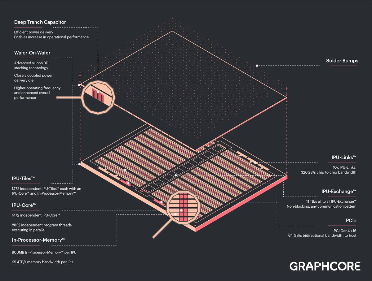
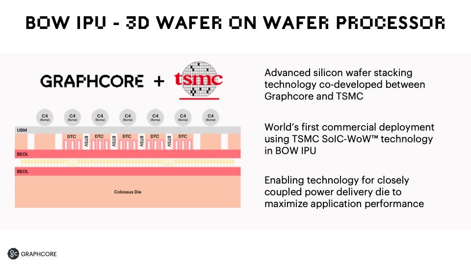
The manufacturing process for Bow involves melding two wafers before the wafers are cut into separate die. The chips are joined via what’s known as “hybrid bonding,” which Knowles likened to cold welding. It joins the metal circuitry of each wafer. The top wafer is then shaved down to a very thin, film-like quality that is “floppy.” The bottom wafer carries the structural support for the two.
Also: AI chip startup Graphcore enters the system business claiming economics vastly better than Nvidia’s
That process makes possible “extremely high density of interconnect between the two wafers,” said Knowles.
It is “more sophisticated,” he said, than typical “chip on wafer” approaches used by, for example, Advanced Micro Devices to bond memory circuits to logic die. Compared to that process, wafer-on-wafer achieves ten times the density of interconnects, he said.
An additional technique in the Bow is a special “via,” a tunnel that connects the stacked die to the rest of the system.
The purpose of the top die that sits on the IPU logic and memory circuits is to bring power to the circuits. Those “deep trench capacitor cells,” as they’re known, are similar to DRAM memory cells. Instead of storing information, the cells a “charge reservoirs” that speed up the logic transistors. That increases the clock speed of transistors from 1.325 gigahertz to 1.85 gigahertz. That results in the 40% speed-up.
The new chip is code-compatible with all existing Graphcore systems, and the company’s Poplar programming environment, and is priced the same as the previous models.
The Bow chip will improve power consumption by 16%, Graphcore said.
The Bow is assembled into IPU-POD machines, called BOW PODs, that scale from 16 Bow chips to 1,024, delivering as much as 358.4 petaflops of compute, in conjunction with up to 64 companion CPU processors.

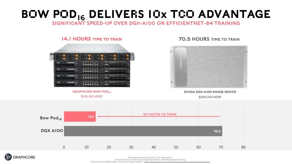
Graphcore, which has demonstrated competitive metrics to Nvidia in benchmark MLPERF tests, claims the BOW POD-16 can deliver a speed up of five times to train the EfficientNet neural network versus a comparable DGX-A100 server from Nvidia. The cost of the BOW POD-16 is half that of the DGX, says Graphcore, $149,995 versus $299,000.
Also: AI startup Graphcore says most of the world won’t train AI, just distill it
Initial customers for the Bow-based Pod machines include Pacific Northwest National Labs, a research laboratory for the U.S. Department of Energy based in Richland, Washington. PNNL are using the machines to run Transformer-based neural networks, and graph neural networks, for tasks such as computational chemistry and cyber-security.
Some partners will offer the Pods as cloud services, including Kingsoft Cloud of China and Cirrascale.
Graphcore co-founder and CEO Nigel Toon, in the same media briefing, said Bow’s wafer-on-wafer approach will make possible many stacked die that will dramatically increase computing power.
“We’re going to leverage this wafer-on-wafer technology to drive the next phase of AI computing,” said Toon.
That next-gen IPU, he said, would realize the vision of 1960s compute scientist Jack Good, a colleague of Alan Turing’s who conceived of an “intelligence explosion.”

Good was the first person to “describe the idea that a computer would be able to exceed the compute capability and the information capacity of a human brain,” said Toon. “We are now embarking, we are working on a project today to deliver this idea of ultra-intelligence.”
“We don’t actually know what that means in terms of computational throughput,” said Knowles. However, there are a few hundred trillion synapses in the human brain.
Those synapses are “very similar to the parameters that are learned by an artificial neural network.” Today’s neural nets have gotten close to a trillion, he noted, “so we clearly have another two or more orders of magnitude to go before we have managed to build an artificial neural network that has similar parametric capacity to a human brain.
Also: Graphcore brings new competition to Nvidia in latest MLPerf AI benchmarks
“This is what we’re announcing today,” said Knowles. “A machine that in fact will exceed the parametric capacity of the human brain.”
“This is not a dream idea, this is a product,” said Knowles. “This is something that we have decided to deliver because our customers have asked for it.
“It’s not intended to be a one off […] and we intend to make many of them and sell them to our customers.”
The Good Computer will combine multiple wafers if logic circuitry, achieving 10 exaflops of compute, 10 billion billion floating point operations per second, fed by four petabytes of memory.
“We expect to be able to deliver this technology as a product for about $120 million,” he said. “It’s a lot of money, but actually, quite a lot less than many of today’s supercomputers.”
Knowles acknowledged that increasingly large neural nets will in future place greater demand on chip-to-chip interconnections. “As model structures get richer, and they start to become more sort-of graph-like, in a sense, there will be constant pressure on inter-chip bandwidth, and certainly that is a factor in our architectural thinking for the follow-on generation.”
For all the latest Technology News Click Here
For the latest news and updates, follow us on Google News.
