


Two-dimensional (2D) semiconductors, such as molybdenum disulfide (MoS2), enable unprecedented opportunities to solve the bottleneck of transistor scaling and to build novel logic circuits with faster speeds, lower power consumption, flexibility and transparency, benefiting from their ultra-thin thickness, dangling-bond-free flat surface and excellent gate controllability.
Tremendous efforts have been devoted to exploring the scaled-up potentials of monolayer MoS2, including both wafer-scale synthesis of high-quality materials and large-area devices. For instance, four-inch wafer-scale monolayer MoS2 with large domain sizes (up to ~300 μm) and record-high electronic quality (average field-effect mobility of ~80 cm2·V-1·s-1) has already been demonstrated via van der Waals epitaxial growth.
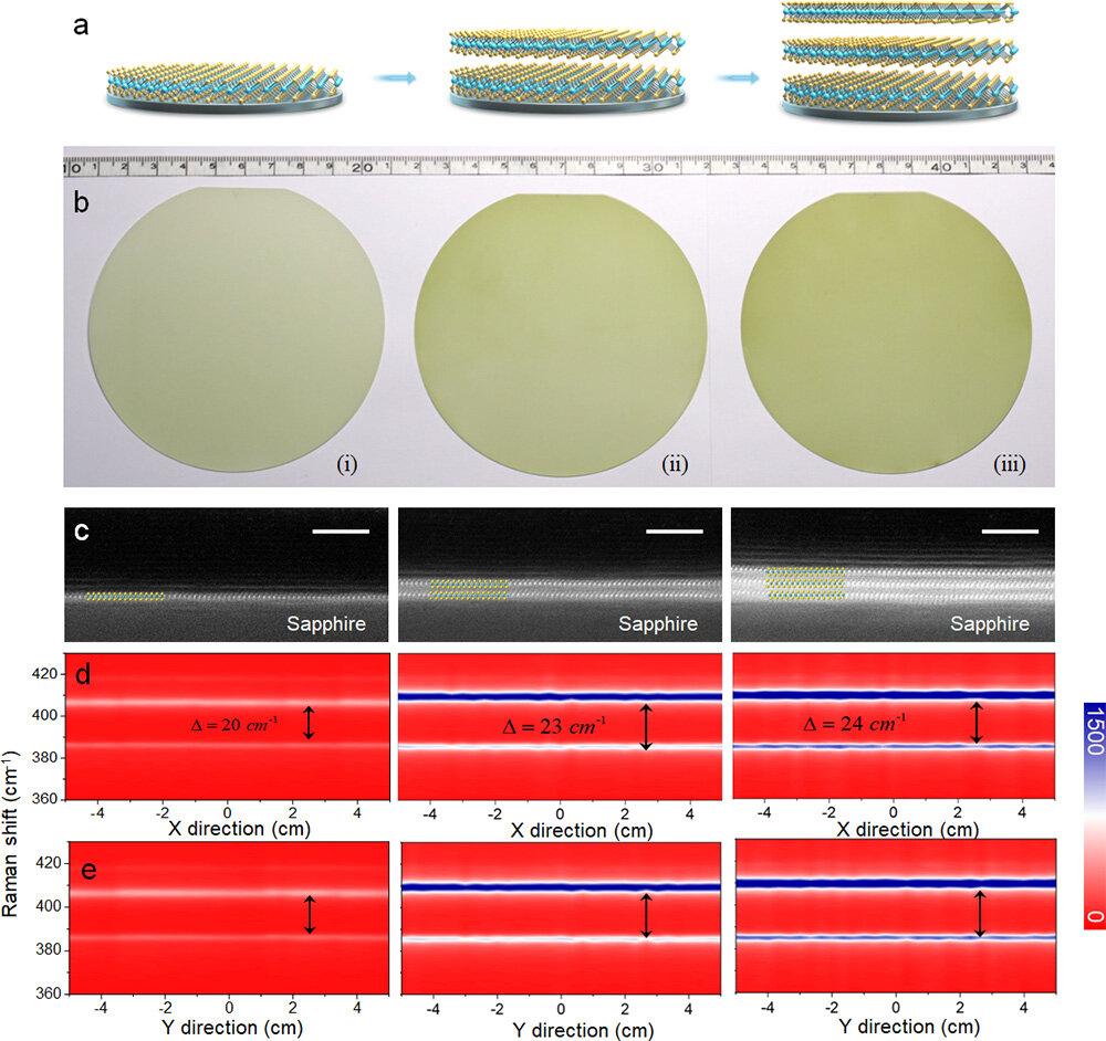
In terms of a further improvement of the electronic quality of the large-scale monolayer MoS2, structural imperfections should be eliminated as much as possible; however, there is not much space left for monolayer MoS2 after ten years of synthesis optimizations in this field. Another key direction is to switch to multilayer MoS2, e.g., bilayers and trilayers, since they have intrinsically higher electronic quality than monolayers and thus are conducive to higher-performance devices and logic circuits. However, due to the fundamental limitation of thermodynamics, it is still a great challenge to realize wafer-scale multilayer MoS2 with high-quality and large-scale uniformity.
Recently, Zhang Guangyu’s group from the Institute of Physics of the Chinese Academy of Sciences (CAS) has overcome the fundamental limitations of thermodynamics by exploiting the proximity effect of a sapphire (0001) substrate and achieved, for the first time, the growth of high-quality multilayer MoS2 four-inch wafers via the layer-by-layer epitaxy process. The epitaxy leads to well-defined stacking orders between adjacent epitaxial layers and offers a delicate control of layer numbers up to six.
Results were published in National Science Review.

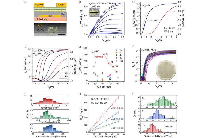
Compared with monolayers, thicker-layer MoS2 field-effect transistors show significant improvements in device performances. For long-channel devices (channel length of five to 50 μm), the average field-effect mobility at room temperature can increase from ~80 cm2·V-1·s-1 for monolayers to ~110/145 cm2·V-1·s-1 for bilayer/trilayer devices, improved by 37.5% / 81.3%.
Considering that, in well-developed thin-film transistors (TFTs), field-effect mobility is 10–40 cm2·V-1·s-1 for indium–gallium–zinc-oxide TFTs and 50–100 cm2·V-1·s-1 for low-temperature polycrystalline silicon TFTs, the excellent average field-effect mobility of >100 cm2·V-1·s-1 strongly uncovers a great potential of bi- and tri-layer MoS2 films for high-performance TFT applications.
In addition, for trilayer MoS2 field-effect transistors, the highest room temperature mobility can reach up to 234.7 cm2·V-1·s-1, setting a new mobility record for devices based on 2D transition-metal sulfide semiconductors.
For devices with a channel length of 100 nm, the current density (Vds=1 V) is increased from 0.4 mA·μm-1 for monolayer to 0.64/0.81 mA·μm-1 for bilayer/trilayer, showing an enhancement factor of 60% / 102.5%. Remarkably, for 40 nm short-channel devices, a record-high on-current densities of 1.70/1.22/0.94 mA/μm at Vds=2/1/0.65 V, as well as a high on/off ratio exceeding 107, are achieved in trilayer MoS2 field-effect transistors.
Such high on-current density of trilayer MoS2 devices outperforms the previous state-of-the-art MoS2 transistors and also exceeds the target of high-performance logic transistors from the International Roadmap for Devices and Systems 2024, moving a step closer to practical applications of 2D MoS2 in electronics and logic circuits at sub-five nm nodes.
Qinqin Wang et al, Layer-by-layer epitaxy of multilayer MoS2 wafers, National Science Review (2022). DOI: 10.1093/nsr/nwac077
Citation:
Epitaxial multilayer MoS2 wafers promise high-performance transistors (2022, June 13)
retrieved 13 June 2022
from https://techxplore.com/news/2022-06-epitaxial-multilayer-mos2-wafers-high-performance.html
This document is subject to copyright. Apart from any fair dealing for the purpose of private study or research, no
part may be reproduced without the written permission. The content is provided for information purposes only.
For all the latest Technology News Click Here
For the latest news and updates, follow us on Google News.