


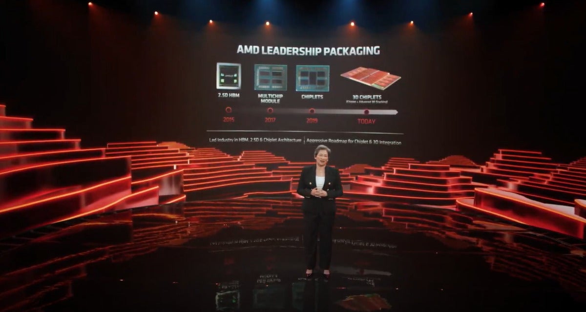
AMD said Monday evening at Computex 2021 that it has evolved its chiplet architecture into 3D chiplets, specifically what it calls 3D V-Cache technology. By itself, the technology promises performance gains for its Ryzen and Epyc processors that can touch 25 percent.
AMD has made “great progress” on its 3D chiplet technology, and should debut it in its “highest-end products” by the end of 2021, AMD chief executive Dr. Lisa Su said during a Computex keynote address.3D V-Cache allows AMD to take a Ryzen 5000 mobile processor and connect a 64MB SRAM cache directly on top of it.
Su showed off a Ryzen 9 5900X, AMD’s fastest gaming CPU, and then compared it to a prototype 5900X with 3D V-Cache attached to it. In Xbox Game Studios’ Gears 5, frame rates improved by 12 percent. In other games, also using an identically clocked 5900X, performance increased 4 to 25 percent, for an average of 14 percent, Su said.
AMD’s Dr. Lisa Su provided benchmarks showing how the prototype 3D V-Cache can dramatically improve gaming performance.
Stacked chips sound like the future
This may all sound familiar. In 2018, Intel began showing off how its Foveros technology allowed for stacking its CPU logic on top of one another. That allowed Intel to create the short-lived Lakefield processor, but also the upcoming, higher-performing Alder Lake chip, which Intel displayed at Computex in both desktop and mobile versions.
AMD CEO Dr. Lisa Su explains 3D V-Cache in her Computex presentation.
According to Tirias Research analyst Kevin Krewell, however, AMD’s implementation of 3D stacking technology is different. AMD is using through-silicon via technology from TSMC, its foundry partner, similar to the technology used by memory makers to stack DRAM and NAND flash on top of one another. It has better power and bandwidth characteristics than Foveros, but it’s unknown how well it can be manufactured.
“AMD is using the tech to get an extra ~12 percent performance boost for its CPUs by adding more L3 cache,” Krewell said via instant message. “This technology can also be used in EPYC servers.”
Placing a large cache directly adjacent to the CPU can have significant performance advantages. Processors need to ask for instructions, and storing them in an easily accessible cache—versus seeking them out in system memory—can be an easy way to increase system performance. But baking that cache into the processor die introduces more opportunity for chip defects. In a worst-case scenario, the entire chip could be rendered useless.
Adding the cache as a separate die and then stacking it saves space and cost, while still maintaining the bandwidth advantage and adding gobs of available cache. For example, Su said its prototype soldered SRAM to each AMD CCD, for a total of 192MB of SRAM cache. The available level-3 cache on today’s 5900X is just 64MB, or a third of the 3D V-Cache prototype.
AMD’s Su holds up the prototype 3D V-Cache chip.
Following AMD’s multichip modules and chiplet approach, Su called 3D chiplets the “next big step forward.” Placing the additional silicon on top of the CPU die triples the available cache. TSMC’s through-silicon vias (or on-chip “wires”) allow the CPU and cache to talk to one another at more than 2 TBps of bandwidth, Su said. Su also said that AMD’s die-to-die approach uses direct copper connections, not solder bumps. That’s an indirect criticism of Intel’s Foveros approach, which uses microbumps and thus consumes more power and provides less bandwidth, Krewell noted.
For now, that also means that AMD can’t easily reproduce Intel’s Alder Lake approach. On the other hand, it might not matter, as AMD can realize performance gains in both its Ryzen and Epyc processors, and possibly its GPUs. Now, the question is: Which of AMD’s chips will be blessed with 3D V-Cache?
For all the latest Technology News Click Here
For the latest news and updates, follow us on Google News.