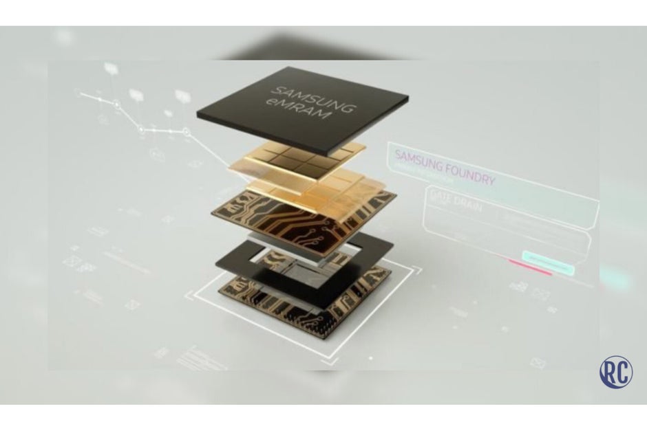
Samsung is first in the world to invent MRAM in-memory computing
Samsung has long been at the forefront of tech innovation, both when it comes to mobile technology and other electronics. The Korean giant just re-affirmed that fact this week, when they became the first company in the world to demonstrate a working in-memory computing process on MRAM.
In devices like smartphones and computers, most of the computing processes are performed by the processing chip, which exists just for this purpose and is highly efficient at it—despite additionally being one of the most power-hungry components.
This memory allows for much faster data transfer with the processor than a storage drive, but also comes in much smaller quantities—such as 4GB, 6GB, or 8GB or 16GB depending on your traditional computing device.
For years now, however, there has been plenty of experimentation with the quest to come up with an efficient and practical in-memory computing solution.
Modern smartphones and computers use DRAM—MRAM is a different animal entirely
Most of the computing devices we interact with from day to day—namely smartphones and computers—run with DRAM, or Dynamic Random Access Memory, as their main memory.
This type of memory is dynamic and volatile, meaning it only stores information as long as the device is powered on with a current flowing through, and it needs to be constantly refreshed or overwritten in order to retain that data.
MRAM, on the other hand—Magnetoresistive Random Access Memory—is a type of non-volatile memory, meaning it can retain bits of data even without an electric current flowing through. It stores memory on magnetic charges, rather than electric charges like standard RAM.
MRAM’s main advantage is its extremely low power usage, although it has faced difficulties in practical integration in modern everyday technology, such as keeping write error rates adequately low. It is also more hostile to in-memory computing than DRAM because of its low resistance.

Samsung’s in-house MRAM, built for the first computer to ever use it as its main memory
The main appeal of in-memory computing as a rule, is that it allows for substantial savings of both time and power. A system which performs at least part of its computing inside the memory, will end up saving all of those milliseconds which it would otherwise take for that data to be requested by the processor, travel to the processor, and be processed there.
Samsung believes that once further developed, MRAM technology will truly shine in processing tasks for artificial intelligence. When tested in AI applications, Samsung demonstrated that its in-memory computing process produced a 93% success rate in picking out specific faces in images, and 98% accuracy in its ability to recognize handwritten numbers.
One of the main authors of Samsung’s research paper, Dr. Seungchul Jung, made the following statement:
“In-memory computing draws similarity to the brain in the sense that in the brain, computing also occurs within the network of biological memories, or synapses, the points where neurons touch one another. In fact, while the computing performed by our MRAM network for now has a different purpose from the computing performed by the brain, such solid-state memory network may in the future be used as a platform to mimic the brain by modeling the brain’s synapse connectivity.”
Samsung hopes that this new invention will be revolutionary in increasing the power efficiency in AI chips more than was ever considered possible before.
For all the latest Technology News Click Here
For the latest news and updates, follow us on Google News.
