
Prof. Becky Peterson at the University of Michigan leads a team that has developed a scalable, manufacturable method for developing thin film transistors (TFTs) that operate at the lowest possible voltage. This is particularly important for TFT integration with today’s silicon complementary metal-oxide semiconductors (CMOS), which are used in the vast majority of integrated circuits.
“We’re essentially developing a less complicated device that operates at lower voltage,” said ECE Ph.D. student Tonglin (Tanya) Newsom, who is first author on the paper. “With this steep sub-threshold swing device, we could significantly lower the energy dissipation of our circuitry, meaning there’s less energy loss. This could help everyone who uses electronic devices.”
TFTs enable the operation of modern displays, acting as switches that control the light at each individual pixel. Switching efficiently between the on and off states allows for lower voltage operation, and results in a more energy-efficient system. One of the key manufacturing challenges to achieving a highly efficient switch is the requirement of a super clean interface between the different material layers within the TFT. A clean interface means electrons can flow in the channel to turn the pixel “on” or “off” without getting trapped.
“The key technology that we were trying to develop is an ultra-clean interface between the semiconductor and the gate insulator, so the switching process between the on and off states would be very sharp,” Peterson said. “We were able to achieve switching at the fastest rate possible, according to fundamental physical limits at room temperature.”
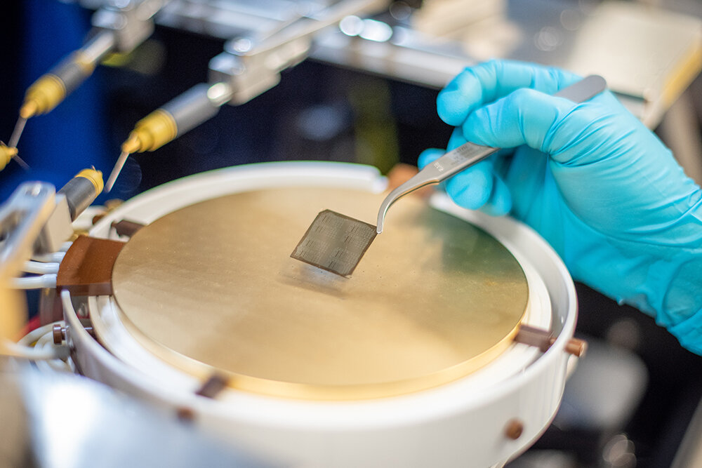
To do this, Peterson’s group partnered with Mechanical Engineering Professor Neil Dasgupta, with whom they developed an atomic layer deposition technology for zinc tin oxide, which is a wide bandgap semiconductor that can be used for electronic and energy devices, such as TFTs, versatile sensors, and solar cells. Peterson’s team took this technology one step further by directly integrating the atomic layer deposition processes for two different key parts of the transistor—the gate capacitor and the semiconductor channel.
“We get the best results by depositing the two layers back-to-back within the same tool, without breaking vacuum,” Peterson said. “This approach demonstrates a straightforward method to achieve optimal TFT performance.”
Peterson’s team focused on amorphous oxide semiconductors, which are a category of materials that are commercialized in displays and enable us to individually control pixels. They’re important for achieving low power operation, high pixel density screens, touch screens, and haptic displays, which generate tactile effects—such as vibrations—for a variety of applications, including wearables and AR/VR devices.
“I truly hope more people will become interested in doing this kind of fundamental science and engineering,” Newsom said “because this work is not just about discovering new possibilities—it’s about improving technology to help the world.”
The research, “59.9 mV·dec-1 Subthreshold Swing Achieved in Zinc Tin Oxide TFTs With In Situ Atomic Layer Deposited Al2O3 Gate Insulator,” was selected as an Editor’s Pick in IEEE Electron Device Letters.
More information:
Tonglin L. Newsom et al, 59.9 mV·dec Subthreshold Swing Achieved in Zinc Tin Oxide TFTs With In Situ Atomic Layer Deposited AlO Gate Insulator, IEEE Electron Device Letters (2022). DOI: 10.1109/LED.2022.3219351
Citation:
Scalable method to manufacture thin film transistors achieves ultra-clean interface (2023, January 26)
retrieved 26 January 2023
from https://techxplore.com/news/2023-01-scalable-method-thin-transistors-ultra-clean.html
This document is subject to copyright. Apart from any fair dealing for the purpose of private study or research, no
part may be reproduced without the written permission. The content is provided for information purposes only.
For all the latest Technology News Click Here
For the latest news and updates, follow us on Google News.