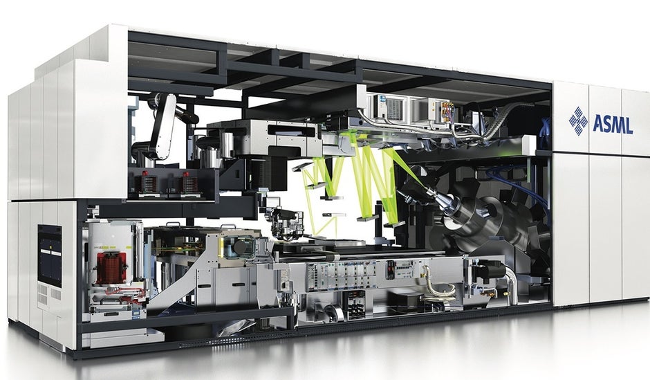
This one $300 million machine will help build powerful chips under 3nm
You might not have ever thought about it, but the smaller the size of the transistors used in chips, the thinner the markings need to be on wafers that show where a chip’s circuitry will be placed. Photo masking used to be the way that circuit patterns were transferred to wafers, but this process was about to be obsolete when Dutch manufacturer ASML created extreme ultraviolet lithography (EUV), a machine that allows extremely thinner patterns to be “printed” on wafers.
ASML’s High NA second-generation EUV will allow foundries to produce chips using a process node under 3nm
High NA actual stands for high numerical aperture. The current EUV machines have an NA of .33, but ASML and ZEISS have been testing machines with an NA of .55.
The higher the NA number, the higher the resolution of the pattern being transferred to a wafer. This could stop foundries from having to run a wafer through the EUV machine a second time to add additional features to a pattern.
These machines focus narrow beams of light on the aforementioned wafers once they have been treated with “photoresist,” a material that is sensitive to light. An ASML spokesman told CNBC about High NA, “It includes a novel optics design and requires significantly faster stages.” The higher resolution will enable 1.7x smaller chip features and 2.9x increased chip density.
The new EUV machines will carry a price tag close to $300 million
And what wasn’t mentioned is that the new machine could reduce the time it takes to bring a chip to market, not a little feature in such a dog-eat-dog industry. But the most important feature is the one mentioned by Chris Miller, an assistant professor at the Fletcher School of Law and Diplomacy at Tufts University. Miller says that the goal with the next-generation EUV machine is to use the narrowest wavelength of light possible in lithography so that the foundries can fit more transistors onto each wafer.
About ASML Miller says, “They’re not resting on their laurels.” He points out that the High NA machine will allow chip designers to create custom patterns on their components.
In 2014 and 2015, customers will be able to use High NA for their own research and development. Starting in 2025, you can expect foundries to use High NA for their high-volume chip manufacturing.
Gartner semiconductor analyst Alan Priestley says that the new EUV machine will allow chip manufacturers to build chips using a process node under 3nm. Right now we are at 5nm with 3nm chips expected to be ready for volume production at the end of next year.
For all the latest Technology News Click Here
For the latest news and updates, follow us on Google News.

