
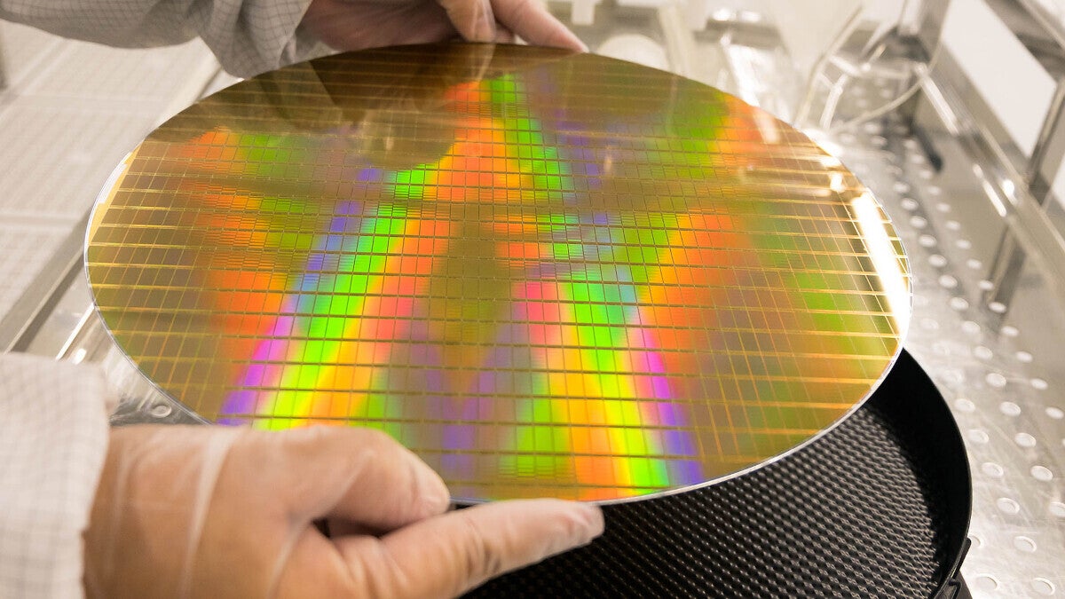
TSMC and Samsung are currently battling each other for control of process leadership. Right now, Samsung Foundry has started shipping chips produced using the 3nm process node. The smaller the node size, the smaller the transistors being used with that particular component. That allows more transistors to fit inside a chip. And the higher the transistor count, usually the more powerful and energy-efficient a chip is.
TSMC’s biggest customer is Apple with the tech giant generating 25% of the foundry’s revenue
For example, in 2016 the Apple A10 Fusion chip was built on TSMC’s 16nm process node and contained 3.3 billion transistors. The iPhone 7 and iPhone 7 Plus each had one of these puppies under their hoods. Let’s move ahead to this year’s iPhone 14 Pro and iPhone 14 Pro Max models which are both powered by the Apple A16 Bionic. The latter is manufactured by TSMC using its enhanced 5nm node which it is calling 4nm, and each chip has close to 16 billion transistors inside.
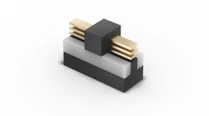
Intel’s RibbonFET transistor could help it take back global process leadership. Image credit-Intel
This chip will be equivalent to 2nm and will use Intel’s new RibbonFET transistors which are more commonly known as GateAllAround (GAA). GAA is already being used by Samsung for its 3nm production and TSMC will use it for its 2nm node. With GAA, current leaks are reduced sharply. Fewer leaks mean that there is less additional power that needs to be made up. GAA is expected to improve performance by 25% with 50% less power consumption.
TSMC is expected to spend over five years on the 3nm and 2nm process nodes
Intel will also use backside power delivery, a feature it calls PowerVia. This would allow transistors to draw power from one side of the wafer while the other side would be used for communications. It would be the first implementation of a system that would eliminate the need for a transistor to route power along the front of a wafer.
For all the latest Technology News Click Here
For the latest news and updates, follow us on Google News.